Newsletter Subscribe
Enter your email address below and subscribe to our newsletter
Enter your email address below and subscribe to our newsletter

 ByJohn A
Power conversion sits at the heart of modern electronics, translating raw electrical energy into stable, usable voltage and current rails. From compact wall chargers and consumer appliances to industrial motor drives and renewable energy inverters, efficient conversion relies on two primary semiconductor functions: rectification and switching.
Rectifiers establish the initial DC stage by routing current in a single direction, while controllable switches modulate energy flow at high frequencies to maintain precise output regulation. Designing a robust power stage requires selecting components that balance conduction losses, thermal management, and switching response across dynamic operating conditions.
Converting alternating current (AC) into direct current (DC) is typically the first hurdle in power supply architectures. This process relies on rectification topologies that convert bi-directional AC waveforms into pulsating DC.
Depending on power level and efficiency goals, designers select specific device structures to optimize forward voltage drop (VF) and reverse leakage current (IR).
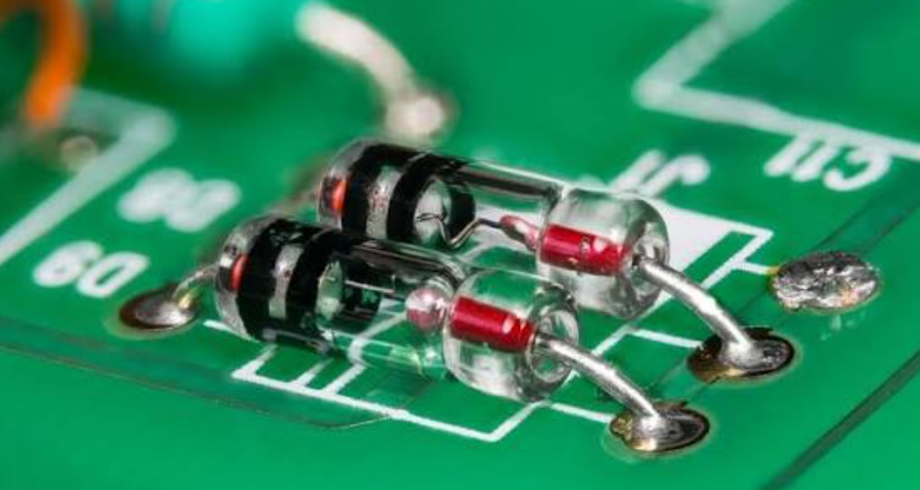
Standard silicon PN junction rectifiers excel in line-frequency (50/60 Hz) applications where conduction losses dominate and switching transitions are slow. However, when handling high-frequency AC outputs—such as those found in secondary stages of switch-mode power supplies (SMPS)—standard diodes suffer from slow reverse recovery times (trr).
Fast-recovery rectifiers utilize targeted gold or platinum doping to speed up minority carrier recombination, drastically reducing switching losses and voltage spikes during high-speed turn-off.
For low-voltage, high-efficiency secondary rectification, Schottky barrier diodes replace the traditional PN junction with a metal-semiconductor barrier. This structural shift eliminates minority carrier storage, yielding virtually instantaneous switching and a significantly lower forward voltage drop (VF≈0.3V to 0.5V).
Schottky devices are crucial for reducing thermal dissipation in battery-powered electronics and high-frequency power converters.
Selecting specialized rectifier components allows hardware designers to fine-tune current handling, breakdown margins, and surge capacities across various circuit topologies.
Once a stable DC bus is established, the system relies on active switches to chop and regulate power at elevated frequencies. Operating at high frequencies allows engineers to shrink passive components like inductors and capacitors, resulting in vastly higher power density.
The choice of switching device depends primarily on system operating voltage, current density, and target switching frequency.
Power MOSFETs are majority-carrier, voltage-controlled devices prized for exceptionally fast switching speeds. Because gate drive current is only required during charging and discharging of parasitic capacitances, control circuitry remains straightforward.
As operating voltages rise above 600V and current requirements push into tens or hundreds of amperes, the RDS(on) of a traditional MOSFET increases significantly. Here, the IGBT becomes the preferred switch.
By pairing a MOSFET-style insulated gate with a bipolar output stage, IGBTs utilize conductivity modulation to maintain a low collector-emitter saturation voltage (VCE(sat)) under heavy load currents. They serve as the core building block for EV traction inverters, industrial motor drives, and solar string inverters.
Engineers evaluating discrete switching options can explore high-performance semiconductor switching devices to match specific gate charge, breakdown voltage, and package thermal requirements.
Even highly efficient semiconductors generate heat during operation due to continuous conduction resistance and dynamic switching transitions. Inadequate thermal dissipation leads to elevated junction temperatures (Tj), accelerated component aging, and thermal runaway.
Packaging plays a central role in directing heat away from the active silicon die to the surrounding environment or secondary cooling assemblies.
Modern compact power supplies rely heavily on surface-mount options like SMA, SMB, SMC, DPAK (TO-252), and D2PAK (TO-263). These packages combine low parasitic inductance with direct thermal pad connections to PCB copper planes, allowing efficient heat spreading across multi-layer boards.
In high-current industrial power stages where external heatsinks or forced-air cooling are required, traditional through-hole packages like TO-220, TO-247, and fully isolated ITO-220 options provide robust mechanical attachment and low junction-to-case thermal resistance (RθJC).
Designing reliable power conversion systems requires a balanced approach to component selection. Rectifiers and controllable power transistors form an interdependent pair: efficient rectification provides a clean, stable DC supply, while fast, low-loss switching devices enable precise regulation and high power density. By carefully evaluating forward conduction drops, switching recovery times, breakdown safety margins, and package thermal performance early in the architecture phase, engineers can build compact, resilient power stages optimized for long-term operational success.